You're about to create your best presentation ever

Integrated Circuit Powerpoint Template

Create your presentation by reusing a template from our community or transition your PowerPoint deck into a visually compelling Prezi presentation.

INTEGRATED CIRCUIT

Transcript: INTEGRATED CIRCUIT INTEGRATED CIRCUIT DEFINITION An integrated circuit (IC), sometimes called a chip, microchip or microelectronic circuit, is a semiconductor wafer on which thousands or millions of tiny resistors, capacitors, diodes and transistors are fabricated. An IC can function as an amplifier, oscillator, timer, counter, logic gate, computer memory, microcontroller or microprocessor.An IC is the fundamental building block of all modern electronic devices. As the name suggests, it's an integrated system of multiple miniaturized and interconnected components embedded into a thin substrate of semiconductor material (usually silicon crystal). A single IC could contain thousands or millions of: Transistors Resistors Capacitors Diodes working The working of an integrated circuit is similar to an amplifier, timer, microprocessor, oscillator, and also computer memory. An IC is made up of Silicon and it is a small wafer that includes thousands of components like resistors, transistors, capacitors, etc. These are small components that can execute different calculations to store data through either analog or digital technology. An IC can function as an amplifier, oscillator, timer, counter, logic gate, computer memory, microcontroller or microprocessor. An IC is the fundamental building block of all modern electronic devices. WORKING APPLICATIONS OF IC: APPLICATIONS Wristwatches Radar Computers Televisions Logic devices Video processors Memory devices. ADVANTAGES ADVANTAGES (i)Extremely small in size, (ii) Low power consumption, (iii) Reliability, (iv) Reduced cost, (v) Very small weight and (vi) Easy replacement. DISADVANTAGES DISADVANTAGES (i)The integrated circuit (IC) can be handle only limited amount of power. (ii)The high grade P-N-P assembly is not possible. (iii)It is difficult to be achieved low temperature coefficient. (iv)The coils or indicators cannot be fabricated. (v)Low noise and high voltage operation are not easily obtained. FUTURE OF IC What is the future of integrated circuit? Nanoelectronics (circuits built with components on the scale of 10 nm) seem to be the most promising successor to lithographic based ICs. Molecular-scale devices including diodes, bistable switches, carbon nanotubes, and nanowires have been fabricated and characterized in chemistry labs.

Integrated Circuit

Transcript: Sources http://www.brighthub.com/engineering/electrical/articles/62185.aspx http://www.google.com/search?tbm=isch&hl=en&source=hp&biw=1024&bih=586&q=integrated+circuit&gbv=2&oq=integrated&aq=0&aqi=g10&aql=&gs_sm=1&gs_upl=882l5959l0l10255l10l10l0l0l0l0l721l3674l3-7.1.0.1l9l0&gs_l=img.1.0.0l10.882l5959l0l10255l10l10l0l0l0l0l721l3674l3-7j1j0j1l9l0 http://www.aztex.biz/general-computer/integrated-circuit-work/ The process of creating Integrated circuits is called Fabrication. Fabrication is a sequence of chemical and photographic steps in which the circuits are constructed on a semiconductor material known as "wafer". a wafer ia a thin slice of semiconductor material used in the fabrication of integrated circuits Steps of Fabrication: Lithography-In this step, a layer of photo-resisting liquid is applied on the surface of semiconductor or wafer. It is then backed and hardened. Etching-In etching process, unwanted material is removed from the wafer. Then the pattern of the photo-resist is transferred to the wafer. Deposition-In this step, films of different materials are applied on the wafer. It is done by either "Physical Vapor Deposition" or "Chemical Vapor Deposition". Oxidation-In the oxidation process, the silicon layers on the top are converted to silicon dioxide by oxygen or water molecules. Diffusion-Diffusion is carried out to anneal the lattice defects. The next step in making an integrated circuit is Packaging. Packaging is also called "encapsulation" or "assembly". It is the final stage of IC manufacturing. In the beginning, ICs were packaged in ceramic flat packs. This technique was used for some years then the "Dual in-line package"(DIP) was introduced. With the passage of time other techniques were introduced such as "Pin Grid Array" and "Surface mount." Intel and AMD have moved to "land Grid array" packages. Today Integrated circuits are mostly packaged in opaque plastic or ceramic insulation. There are metal pins in the packaging which are used to connect to the outside world. How Is it made A circuit is a path we electric currents or pulses flow Integrated circuits are in almost every appliance known to man at this point in history from wristwatches to televisions and from coffee makers to, the most obvious, computers. An integrated circuit is a collection of diodes, transistors and microprocessors in miniature scale all operating on a single piece of semiconductor. The semiconductor is most of the time made from silicon. Diodes control how much, when and how often electrons or electricity is allowed to flow into other parts of the system. Transistors can store voltage to stabilize the circuit or for amplifying a signal. A transistor can be used as a switch, similar to a light switch, for an integrated circuit or for functions held within the circuit. The most important part of an integrated circuit is the microprocesser.Microprocessors simply give the integrated circuit memory, memory to perform calculations and follow logic, or a set of rules Pictures of integrated circuit Integrated Circuit How it works

Integrated Circuit

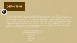
Transcript: Question & Hypothesis "What happens to the electric current(A) when the potential(V) gets bigger? "If potential gets bigger, then electric current also gets bigger.' The Materials TI-Nspire, lab cradle, regulated DC power supply, 3 different type resistors, voltage probe and a current sensor. IC The question set before the experiment was "What happens to the electric current when the potential gets bigger?" After the Ohm's Law experiment finished, the graph and data show certain a relationship between the potential and the current. All of the three different graphs draws a rising curve. This means, when the potential increases, the current also increases. The potential and the current are in direct proportional relationship. According to result of the experiment, the hypothesis is proven correct because it states, "if the potential gets bigger, then electric current also gets bigger." *Photolithography: It is process of transferring geometric shapes on a mask to the surface of a silicon wafer. Integrated circuits were invented in 1958 by Jack Kilby, who was an engineer of Texas instruments. He demonstrated successfully the first working integrated circuit device. One and a half years after Kilby demonstrated his IC design, Robert Noyce of Fairchild Semiconductor Limited came up with his own integrated circuit. His model solved many practical problems which Kilby's device had. The earlier developed IC's had only few transistors and resistors on the chip. In the early 1960's SSI(Small Scale Integration) circuits were manufactured. SSI circuits consisted of few tens of components on the chip. Further development in the mid 70's led to LSI(Large Scale Integration), devices which had thousands of transistors per chip. 1KB RAM is an example of a LSI. Then, in early 80's VLSI(Very Large Scale Integration) was introduced. Today we have very complex devices such as ULSI(Ultra Large Scale Integration), SOC(System On Chip), WSI(Waferscale Integration), and 3D-IC(Three dimensional Integrated Circuits). History of Integrated Circuit Before the Ohm's Law experiment... Data & Graph of Ohm's law experiment The IC has two main advantages: cost and performance. Cost is low because the chips, with all their components, are printed as a unit by photolithography rather than being constructed on a transistor one at a time. Performance is high because the IC's components switch quickly and consume little power as a result of the small size and close proximity of the components. After all the materials which are needed for experiment are collected, set up the DC power supply, resistor, voltage probe, current sensor on the table, and connect resistor to regulated DC power supply, voltage probe and current sensor in right order. After that, read the TI-Nspire and check the current and the potential are not in minus. Then, start to increase the potential using DC power supply. Continue increasing for 5 seconds. After, record your data and graph in the TI-Nspire, change the resistor to different one and repeat it again. Information of What is integrated Circuit? How and for what purpose it is used? Who is the inventor of it? How it improved in the past? What is ohm's law? What is the purpose of ohm's law experiment? Who are you? Integrated Circuit Conclusion Thank you! An integrated circuit, IC, is a keystone of modern electronics. It is the heart and brains of most circuits, and set of electronics circuits on one small plate of semiconductor material. It is the ubiquitous little black 'chip' you find on just about every circuit board. It is normally made of silicon. You may cannot see this text. If you see this text, just ignore it. Integrated circuits are used in virtually all electronic equipment today and have revolutionized the world of electronics. Computers, mobile phones, and other digital home appliances are now inextricable parts of the structure of modern societies, made possible by the low cost of integrated circuits. "Everything" about Integrated Circuit "Integrated Circuits." Electrical4u. N.p., n.d. Web. 07 Apr. 2015. <http://electrical4u.com/integrated-circuits-types-of-ic/>. "Integrated Circuits." Sparkfun. N.p., n.d. Web. 07 Apr. 2015. <https://learn.sparkfun.com/tutorials/integrated-circuits>. Keating, Bernie. "Electronics." A Romp Thru Science: Plato and Einstein to Steve Jobs. Bloomington: AuthorHouse, 2012. N. pag. Web. 7 Apr. 2015. Uber, Alessandro. "Integrated Circuit." PhysicalTimingClosure.com. N.p., n.d. Web. 09 Apr. 2015. <http://physicaltimingclosure.com/docs_ic.html>. Procedure of Experiment Works Cited Where are we use ICs? What is an Integrated Circuit? Why are we use ICs?

Integrated circuit

Transcript: integrated circuit by Giuseppe cuddemi Integrated circuit are complex circuit that contain thousand or millions of resistors and capacitors and diodes, all inside one package. What are? How they are made? 7 step: Wafers Oxidation Photo-lithography Etching Doping Depositing films Testing and Packaging first, A silicon substrate is created by silicing a rod-shaped, ultrapure silicon crystal into round wafers. In the next step, oxidation, an insulating layer, called a dielectric, is placed on the silicon substrate by exposing the wafer to oxygen in a furnace at abaut 1.000° C. A thin Layer of oxide is formed on the surface of the wafer,which is then covered with a film of light-sensitive. material called photorestist. when exposed to light, this material becomes easy to dissolve then the wafer is etched: the exposed areas of photoresist and the oxide layer beneath them are removed either by chemicals, or by exposure to a corrosive gas, called a plasma, in a special vacuum chamber. The next step is doping. impurities are introduced into the exposed silicon to alter its conductivity and form negative and positive conducting zones. TO complete the integrated structure, it is necessary to deposit various films and repeat the steps used to pattern them. films are deposited in 3 ways: -by using sputterers -by evaporation -by chemical vapour deposition The finished chips are tested before packaging using automated test equipment. the wafer is then cut into blocks, called dies, and the defective ones are discarded. ICs come in a wide variety of packages and sizes. they are mounted on printed circuit board for interconnection with other circuits or components. Different type of ICs Flat packs The circuits are hermetically sealed in flat packs. ICs are used by military for their reliability and small size. The dual in-line package is a package with a rectangular housing and two parallel rows of downward-pointing connecting pins. dip The pin grid array is a package with one face covered with pins in a grid pattern. pga The ball grid array derive from the PGA. The pins are replaced by balls of solder stuck to the bottom of the package. bga A System in Package is a number of ICs enclosed in a single package. sip Characteristics ICs can be : ANALOG (Linear) work by processing continuous signals. DIGITAL work using binary mathematics to process "one" and "zero" signals. They are combined to create functions such as A/D converters and D/A converters. scale integration ICs are classified by the number of electronic components they contain. There are five type of scale integration. ssi The first integrated circuits manufactured in 1960s were called "Small-Scale integration" and contained up to 100 electronic components per chip. msi The next step introduced devices called "Medium-Scale Integration" which contained from 100 to 3.000 electronic components per chip. lsi Further development led to "Large-Scale Integration" in the mid 1970s, with 3000 to 100.000 electronic components per chip. vlsi The final step in the development process, which started in 1980s, was "Very Large-Scale Integration" with 100.000 to 1.000.000 electronic components per chip. ulsi The term "Ultra-Large-Scale Integration" was proposed for chip with more then one million of transistors. doping The doping of a semiconductor is the adding of a substance, an impurity, into its crystal lattice in order to change its conductivity. P-doped silicon N-doped silicon

integrated circuit

Transcript: Steps to make a chip Produce an IC is very expensive. But with only one chip, a several hundred of integrated circuits are made, so it become an advantage. The performance of IC is high and consume little power, being small and close together. ICs are classified by the number of electronic components they contain. The first is the “Small Scale Integration” (SSI) and contained up to 100 electronic components. They were used in Apollo program. Small-Scale Integration Depositing on a film 3 Medium -Scale Integration System in package (SIP) It is a number of ICs enclosed on a single package. It has the same function of an electronic system. It is used in mobile phones and digital music players. Unfortunately, any defected chip in the package will result a failure for the microchip. Ball grid array (BGA) It is a package like the PGA but the pins are replaced by balls of solder stuck to the bottom of the package. It is paced on a PCB that carries the copper pads in a pattern that matches the solder balls. Then the assembly is heated and solidifies. An insulating layer is placed on the silicon substrate. It is possible by exposing the wafer to oxygen in a furnace at 1’000 °C. Then this layer of oxide is covered with a film of light-sensitive material called photoresist Jack Kilby The first integrated circuit was developed in the 1950s by Jack Kilby and Robert Noiyce APE Flat packs They were hermetically sealed packages. Now they are used by military for their reliability and small size. A silicon substrate is created by slicing a rod-shaped ultrapure silicon crystal into round wafer. Then it is polished to give it a smooth mirror-like surface Impurities are introduced into the exposed silicon to alter its conductivity and form negative and positive conducting zones. This may be carried out by diffusion or ion-implantation Finally the chip are tested with APE (automated test equipment) and if the test is OK they are packaged Robert Noiyce Pin grid array (PGA) It is a package with one face covered with pins in a grid pattern. Thanks to the space of 2.54 mm with the pins you can insert it into the holes in a printed circuit board. This type occupies less space than the DIP. The film may be deposed in 3 ways: • Using sputterers in which thin films are grown in plasma (1) • By chemical vapour deposition (2) • By evaporation (3) 2 Oxidation They stated to be developed in the mid of 1979s and they contain from 3000 to 100000 electronic components per chip. The first microprocessor had under 4000 transistors and LSI circuit began to be produced in 1974 for computer main memories and second-generation of microprocessors ICs or microchips are complex circuit that contain millions of electronic components like transistors, diodes, resistors, capacitors inside one package Integrated circuits are the most important components in computing, communications, transport systems. And scientists think that the developed of ICs is one of the most important events in the history of mankind Slicing integrated circuit Microchips can be contained into different packages Doping Large -Scale Integration Very Large -Scale Integration Cost and performance of ICs Etching Analogue ICs , such as sensors, work by processing continuous signals. On the contrary digital systems work using binary scale to process “one” and “zero” signals. They can also combine analogue circuits and digital circuits to create de function of A/D converts and D/A converts. The wafer is exposed to ultraviolet light through a mask that reproduces the circuit patterns. This way every layer on the wafer is patterned into the shape of the circuit elements. Final test and packaging http://www.intel.com/content/dam/www/public/us/en/documents/packaging-databooks/packaging-chapter-14-databook.pdf Dual in-line packages (DIP) It is a package with a rectangular housing and two parallels rows of pins. The pins are set at a standard distance and they are numbered anti-clockwise These devices contain from 100000 to 1 million electronic components. For the first time a CPU was fabricate on a single chip to create microprocessor. Finally it was introduced the term “ULSI” (ultra Large -Scale Integration) for marketing. Photolithography These devices contain from 100 to 3’000 electronic components. The cost are little more than SSI but they made it possible to manufacture much more complex systems. 1 This step consist of etched the wafer, so the exposed areas of photoresist are removed by chemicals or by exposure to a corrosive gas Analogue and digital ICs

Now you can make any subject more engaging and memorable